


Popular in your industry


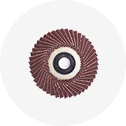
4.5" Diamond Flap Disc Flap Sanding Disc Diamond Electroplated Grit 60 For Angle Grinder Dry Wet Use


Chemical Vapor Deposition (CVD) diamond wafers represent a pinnacle of technological advancement in synthetic diamond production. These wafers are crafted through a sophisticated process where gases are utilized to deposit diamond onto a substrate, allowing for the creation of high-purity diamond layers. The versatility of CVD diamond wafer applications spans across various industries, from electronics to cutting-edge research.
The utility of CVD diamond wafers is vast, with each type serving a specific industrial need. In electronics, they are essential for heat sinks and semiconductors due to their excellent thermal conductivity. The medical field employs them in radiation detection devices, while in optics, they are used for high-power laser windows and lenses. Each application benefits from the wafer's superior hardness and thermal properties.
A CVD diamond wafer is distinguished by its exceptional hardness and thermal conductivity, making it ideal for tasks that require precision and durability. The material composition of these wafers is pure synthetic diamond, which provides a consistency in quality that is unmatched by natural diamonds. This uniformity is crucial for applications requiring predictable performance and reliability.
The advantages of utilizing CVD diamond wafers are manifold. Their resistance to wear and tear is unparalleled, ensuring longevity in applications where lesser materials would fail. The wafers' thermal properties also allow for efficient heat dissipation, which is critical in high-performance electronic devices. Additionally, their optical clarity is beneficial for laser systems, where any impurity can significantly degrade performance.
Selecting the appropriate CVD diamond wafer involves considering factors such as grain size, purity, and thermal conductivity. The intended use dictates the specifications required, with different applications necessitating variations in wafer properties. For instance, a wafer used in high-frequency electronic devices would prioritize thermal conductivity, while one used in optics would focus on clarity and purity.
Alibaba.com serves as a gateway for businesses to source CVD diamond wafers tailored to their specific needs. With a comprehensive assortment of wafers, the platform connects buyers with reputable suppliers, facilitating the acquisition of materials that meet their precise requirements. The emphasis is on providing a diverse range of options to suit the multifaceted demands of modern industries.


 浙公网安备 33010002000092号
 浙B2-20120091-4